CBSE Class 12 · 1997 · SemiconductorsVery Short Answer

WhatsApp Email
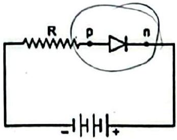
Draw a p-n junction with reverse bias.

Solution

To reverse bias a junction diode, connect the p-region to the negative terminal and the n-region to the positive terminal of the external battery.
The external field then aids the junction field, so the potential barrier and the width of the depletion layer both increase, and only a small reverse (minority-carrier) current flows.

CBSE Class 12 Board · 1997 · Subjective

More board questions on Semiconductors

  1. A pure Si crystal having atoms is doped with 1 ppm concentration of antimony. If the concentration of holes in the doped crystal is found to be , the concentration (in ) of intrinsic charge carr …
    CBSE 2024View solution →
  2. (a) Explain the characteristics of a p-n junction diode that makes it suitable for its use as a rectifier.
    (b) With the help of a circuit diagram, explain the working of a full wave rectifier.
    CBSE 2024View solution →
  3. Explain the following, giving reasons.
    (a) A doped semiconductor is electrically neutral.
    (b) In a p-n junction under equilibrium, there is no net current.
    (c) In a diode, the reverse current is practically independent of the applied voltage.
    CBSE 2024View solution →
  4. In an extrinsic semiconductor, the number density of holes is . If the number density of intrinsic carriers is , the number density of electrons in it is
    CBSE 2023View solution →
  5. Pieces of copper and of silicon are initially at room temperature. Both are heated to temperature T. The conductivity of
    CBSE 2023View solution →
  6. The formation of depletion region in a p-n junction diode is due to
    CBSE 2023View solution →