Define the terms 'potential barrier' and 'depletion region' for a p-n junction diode.
Solution
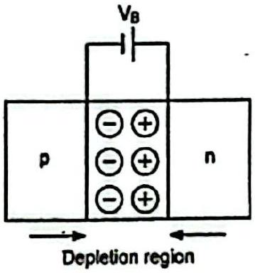
During junction formation, diffusion leaves immobile negative ions on the p-side and positive ions on the n-side. The resulting potential difference across the junction, which opposes further diffusion of majority carriers, is the potential barrier (~0.3 V for Ge, ~0.7 V for Si). The thin carrier-free layer containing only these immobile ions is the depletion region (~1μm wide). Barrier opposes diffusion; depletion layer is carrier-free.