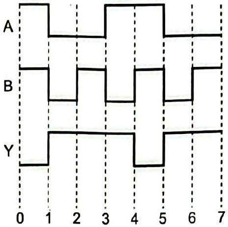
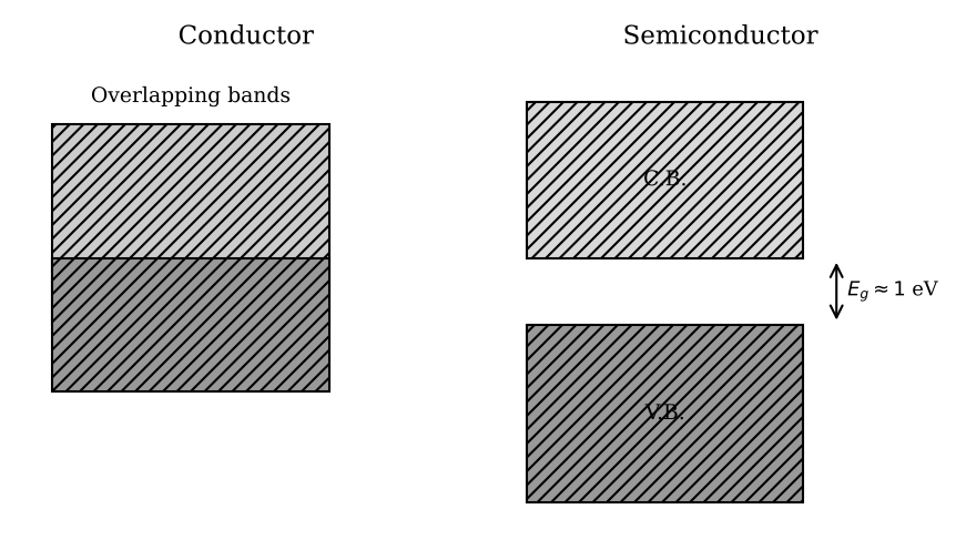
(i) Distinguish between a conductor and a semiconductor on the basis of energy band diagram. (ii) The figure shows the input waveforms (A, B) and the output waveform (Y) of a gate. Identify the gate, write its truth table and draw its logic symbol.
Solution
(i) In a conductor the valence and conduction bands overlap (or the conduction band is partly filled), so there is no forbidden gap and conduction is easy. In a semiconductor a small forbidden gap (≈1eV) separates a filled valence band from an empty conduction band, so only a few carriers are available at room temperature. (ii) Reading the waveforms: (A,B)=(1,1)→Y=0 and all other combinations give Y=1. This is the NAND operation Y=A⋅B; its symbol is an AND symbol with an output bubble. (i) overlap vs small gap; (ii) NAND gate.
CBSE Class 12 Board · 2016 · All India · Subjective