CBSE Class 12 · 2015 · Delhi · SemiconductorsShort Answer

WhatsApp Email
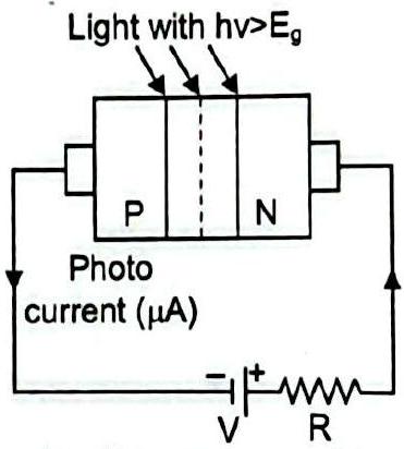
With what considerations in view is a photodiode fabricated? State its working with the help of a suitable diagram. Even though the current in forward bias is known to be more than in reverse bias, the photodiode works in reverse bias — what is the reason?

Solution

Fabrication considerations: the junction is made with a transparent window so that light reaches the depletion region, and the material's band gap is chosen so that the photons to be detected have .
Working: in reverse bias, incident photons generate electron-hole pairs in the depletion region; these are swept across the junction, producing a reverse photocurrent proportional to the incident light intensity.
Reason for reverse bias: on illumination the fractional change in the small reverse (minority-carrier) current is large and easily measured, whereas the already large forward current changes negligibly.

CBSE Class 12 Board · 2015 · Delhi · Subjective

More board questions on Semiconductors

  1. A pure Si crystal having atoms is doped with 1 ppm concentration of antimony. If the concentration of holes in the doped crystal is found to be , the concentration (in ) of intrinsic charge carr …
    CBSE 2024View solution →
  2. (a) Explain the characteristics of a p-n junction diode that makes it suitable for its use as a rectifier.
    (b) With the help of a circuit diagram, explain the working of a full wave rectifier.
    CBSE 2024View solution →
  3. Explain the following, giving reasons.
    (a) A doped semiconductor is electrically neutral.
    (b) In a p-n junction under equilibrium, there is no net current.
    (c) In a diode, the reverse current is practically independent of the applied voltage.
    CBSE 2024View solution →
  4. In an extrinsic semiconductor, the number density of holes is . If the number density of intrinsic carriers is , the number density of electrons in it is
    CBSE 2023View solution →
  5. Pieces of copper and of silicon are initially at room temperature. Both are heated to temperature T. The conductivity of
    CBSE 2023View solution →
  6. The formation of depletion region in a p-n junction diode is due to
    CBSE 2023View solution →