CBSE Class 12 · 2016 · Delhi · SemiconductorsShort Answer

WhatsApp Email
(a) Write the functions of the three segments of a transistor.
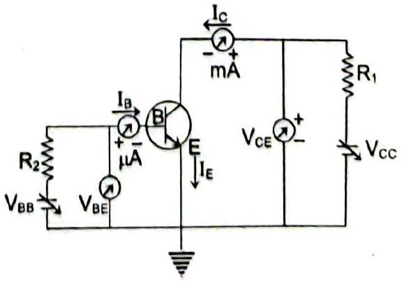
(b) Draw the circuit diagram for studying the input and output characteristics of an n-p-n transistor in common emitter configuration, and explain how the input and output characteristics are obtained.

Solution

(a) The emitter is heavily doped and supplies the majority charge carriers; the base is thin and lightly doped and controls the fraction of carriers reaching the collector; the collector is moderately doped and larger in size, and collects the carriers.
(b) Connect the n-p-n transistor in CE configuration with a source (with a resistor) for the base and for the collector, and meters to read , , and .
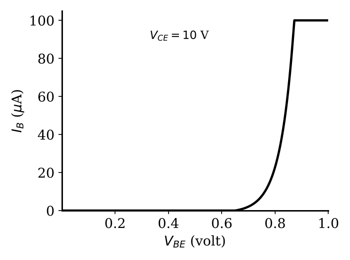
Input characteristic: keep fixed and plot against .
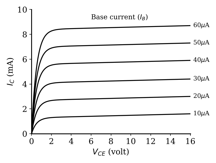
Output characteristic: keep fixed and plot against , repeating for several values of .

CBSE Class 12 Board · 2016 · Delhi · Subjective

More board questions on Semiconductors

  1. A pure Si crystal having atoms is doped with 1 ppm concentration of antimony. If the concentration of holes in the doped crystal is found to be , the concentration (in ) of intrinsic charge carr …
    CBSE 2024View solution →
  2. (a) Explain the characteristics of a p-n junction diode that makes it suitable for its use as a rectifier.
    (b) With the help of a circuit diagram, explain the working of a full wave rectifier.
    CBSE 2024View solution →
  3. Explain the following, giving reasons.
    (a) A doped semiconductor is electrically neutral.
    (b) In a p-n junction under equilibrium, there is no net current.
    (c) In a diode, the reverse current is practically independent of the applied voltage.
    CBSE 2024View solution →
  4. In an extrinsic semiconductor, the number density of holes is . If the number density of intrinsic carriers is , the number density of electrons in it is
    CBSE 2023View solution →
  5. Pieces of copper and of silicon are initially at room temperature. Both are heated to temperature T. The conductivity of
    CBSE 2023View solution →
  6. The formation of depletion region in a p-n junction diode is due to
    CBSE 2023View solution →