CBSE Class 12 · 2006 · All India · SemiconductorsLong Answer

WhatsApp Email
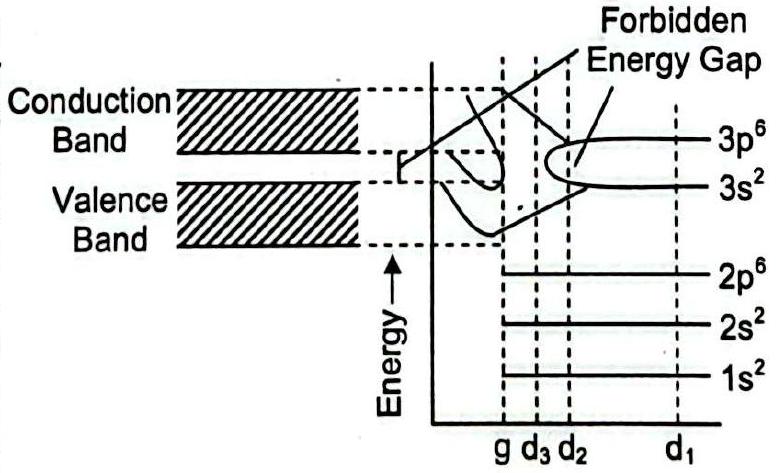
What are energy bands? How are these formed? Distinguish between a conductor, an insulator and a semiconductor on the basis of energy band diagram.

Solution

A free atom has sharp, discrete energy levels.
When atoms form a crystal, each level splits into very closely spaced levels because of the interaction between neighbouring atoms; these closely packed levels constitute an energy band.
The outer levels form the valence band (highest filled) and the conduction band (next, usually empty), separated by the forbidden gap .
Conductor: the conduction and valence bands overlap (or the conduction band is partly filled), so conduction is easy.
Insulator: a large gap () keeps the conduction band empty, so conduction is negligible.
Semiconductor: a small gap () allows a few electrons to be thermally excited into the conduction band.

CBSE Class 12 Board · 2006 · All India · Subjective
More board questions on Semiconductors

  1. A pure Si crystal having atoms is doped with 1 ppm concentration of antimony. If the concentration of holes in the doped crystal is found to be , the concentration (in ) of intrinsic charge carr …
    CBSE 2024View solution →
  2. (a) Explain the characteristics of a p-n junction diode that makes it suitable for its use as a rectifier.
    (b) With the help of a circuit diagram, explain the working of a full wave rectifier.
    CBSE 2024View solution →
  3. Explain the following, giving reasons.
    (a) A doped semiconductor is electrically neutral.
    (b) In a p-n junction under equilibrium, there is no net current.
    (c) In a diode, the reverse current is practically independent of the applied voltage.
    CBSE 2024View solution →
  4. In an extrinsic semiconductor, the number density of holes is . If the number density of intrinsic carriers is , the number density of electrons in it is
    CBSE 2023View solution →
  5. Pieces of copper and of silicon are initially at room temperature. Both are heated to temperature T. The conductivity of
    CBSE 2023View solution →
  6. The formation of depletion region in a p-n junction diode is due to
    CBSE 2023View solution →