JEE Main · 2008 · 27 Apr 2008 · Offline · Semiconductors

WhatsApp Email
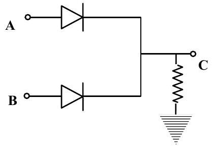
In the circuit below, A and B represent two inputs and C represents the output. The circuit represents
  1. (A)NOR gate
  2. (B)AND gate
  3. (C)NAND gate
  4. (D)OR gate✓ Correct

Answer: (D)

Solution

Reading the diode network, each input is tied to the output through a diode arranged so that a high level at either input drives the common output high. If or or both is at logic , the corresponding diode conducts and pulls up to ; only when both inputs are held at does the output stay at . An output that is high whenever any input is high is exactly the behaviour of an OR gate.

JEE Main · 2008 · 27 Apr 2008 · Offline · Single correct option
More JEE Main questions on Semiconductors

  1. Find the correct combination of A, B, C and D inputs which can cause the LED to glow.
    JEE Main 2026View solution →
  2. For the given logic gate circuit, which of the following is the correct truth table?
    JEE Main 2026View solution →
  3. A voltage regulating circuit consisting of Zener diode, having break-down voltage of 10 V and maximum power dissipation of 0.4 W, is operated at 15 V. The approximate value of protective resistance in this circuit is ______ .
    JEE Main 2026View solution →
  4. Identify the correct truth table of the given logical circuit.
    JEE Main 2026View solution →
  5. Two p-n junction diodes and are connected as shown in figure. A and B are input signals and C is the output. The given circuit will function as a ______.
    JEE Main 2026View solution →
  6. The given circuit works as :
    JEE Main 2026View solution →