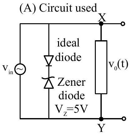
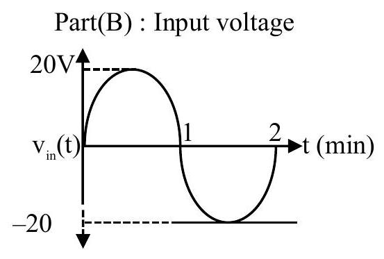
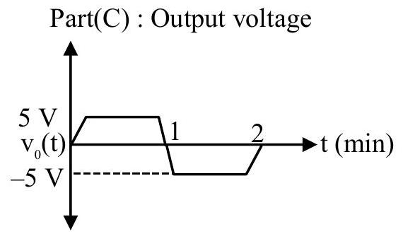
For the given circuit (shown in part (A)) the time dependent input voltage vin (t) and corresponding output vo(t) are shown in part (B) and part (C), respectively. Identify the components that are used in the circuit between points X and Y.ABC
(A)(see structure)
(B)(see structure)✓ Correct
(C)(see structure)
(D)(see structure)
Answer: (B)
Solution
On the positive half-cycle the top rail goes positive, forward biasing the middle-branch ideal diode while its Zener holds in breakdown, so the output is clamped to +5 V; the branch across X and Y must stay non-conducting here. On the negative half-cycle the middle-branch diode is reverse biased and that branch is open, so the branch across X and Y must now conduct and hold the output at −5 V through its own Zener breakdown. This requires, between X and Y, an ideal diode in series with a Zener diode set to the opposite polarity of the middle branch, with their anodes joined so the pair conducts only on the negative half-cycle and clamps at 5 V, reproducing the flat ±5 V output. The components between X and Y are an ideal diode in series with a Zener diode arranged back to back with the middle branch.
JEE Main · 2026 · 02 Apr 2026 · Shift 1 · Single correct option