JEE Main · 2025 · 22 Jan 2025 · Shift 2 · Semiconductors

WhatsApp Email
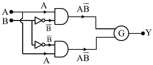
To obtain the given truth table, following logic gate should be placed at G :
  1. (A)NOR Gate✓ Correct
  2. (B)AND Gate
  3. (C)NAND Gate
  4. (D)OR Gate

Answer: (A)

Solution

Inputs A and B first pass through a NOT-then-AND stage: the top AND gate takes A and , giving ; the bottom AND gate takes and B, giving . These two signals P and Q are the actual inputs to gate G, not A and B directly.

Evaluating P and Q for each row of the given table:
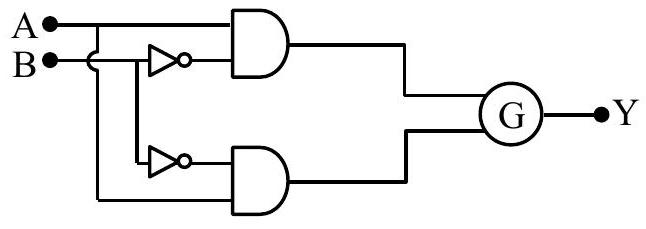
A=0, B=0: P = 0·1 = 0, Q = 1·0 = 0
A=0, B=1: P = 0·0 = 0, Q = 1·1 = 1
A=1, B=0: P = 1·1 = 1, Q = 0·0 = 0
A=1, B=1: P = 1·0 = 0, Q = 0·1 = 0

So (P,Q) takes the values (0,0), (0,1), (1,0), (0,0) across the four rows, and the required outputs are Y = 1, 0, 0, 1 respectively.

Testing a NOR gate at G, :
(0,0) → 1, (0,1) → 0, (1,0) → 0, (1,1) → 0

This reproduces Y = 1, 0, 0, 1 for every row of the table exactly, so gate G is a NOR gate.

JEE Main · 2025 · 22 Jan 2025 · Shift 2 · Single correct option

More JEE Main questions on Semiconductors

  1. Find the correct combination of A, B, C and D inputs which can cause the LED to glow.
    JEE Main 2026View solution →
  2. For the given logic gate circuit, which of the following is the correct truth table?
    JEE Main 2026View solution →
  3. A voltage regulating circuit consisting of Zener diode, having break-down voltage of 10 V and maximum power dissipation of 0.4 W, is operated at 15 V. The approximate value of protective resistance in this circuit is ______ .
    JEE Main 2026View solution →
  4. Identify the correct truth table of the given logical circuit.
    JEE Main 2026View solution →
  5. Two p-n junction diodes and are connected as shown in figure. A and B are input signals and C is the output. The given circuit will function as a ______.
    JEE Main 2026View solution →
  6. The given circuit works as :
    JEE Main 2026View solution →