JEE Main · 2025 · 02 Apr 2025 · Shift 2 · Semiconductors

WhatsApp Email
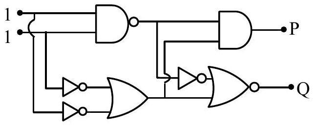
In the digital circuit shown in the figure, for the given inputs the P and Q values are :
  1. (A)
  2. (B)✓ Correct
  3. (C)
  4. (D)

Answer: (B)

Solution

Both inputs are . The first gate is a NAND, and ; this is fed to the AND gate whose output is P, so regardless of its other input. Each input line is also inverted to and fed to the lower NOR gate, giving ; this reaches the final NOR gate that produces Q, and a NOR gate with any input equal to gives output , so . The outputs are and .

JEE Main · 2025 · 02 Apr 2025 · Shift 2 · Single correct option
More JEE Main questions on Semiconductors

  1. Find the correct combination of A, B, C and D inputs which can cause the LED to glow.
    JEE Main 2026View solution →
  2. For the given logic gate circuit, which of the following is the correct truth table?
    JEE Main 2026View solution →
  3. A voltage regulating circuit consisting of Zener diode, having break-down voltage of 10 V and maximum power dissipation of 0.4 W, is operated at 15 V. The approximate value of protective resistance in this circuit is ______ .
    JEE Main 2026View solution →
  4. Identify the correct truth table of the given logical circuit.
    JEE Main 2026View solution →
  5. Two p-n junction diodes and are connected as shown in figure. A and B are input signals and C is the output. The given circuit will function as a ______.
    JEE Main 2026View solution →
  6. The given circuit works as :
    JEE Main 2026View solution →